


Quantum Nano-spintronics Laboratory
Section of technologies and diagnostics of nanostructures
|
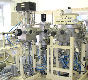
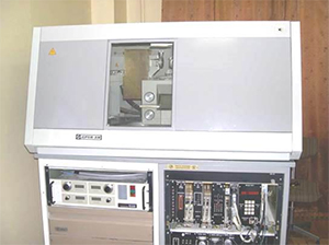
High vacuum precision magnetron machine MPS-4000-C6 (ULVAC Inc., Japan). It is used for the preparation of multilayer nanostructures with metallic and dielectric layers: magnetic metallic superlattices and spin valves with giant magnetoresistive effect, as well as spin-tunnel nanostructures with MgO dielectric.
Main characteristics:
|
|
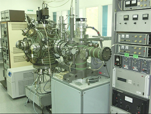
Ultrahigh vacuum molecular beam epitaxy unit "Katun-S". It allows the growth of thin single-crystal metal films and multilayer magnetic nanostructures.
Main characteristics:
|
|
Automated vibrating magnetometer AVM-1 (IMP Ural Branch of RAS, Ekaterinburg). It is designed to study at room temperature the magnetic characteristics of massive samples, thin magnetic films and multilayer nanostructures.
Main characteristics:
|
|
Automated setup RTF-1 (IMP Ural Branch of RAS, Ekaterinburg). It is designed to measure temperature dependences of resistance (on direct current) in a given magnetic field and field dependences of magnetoresistance at a fixed temperature of both massive and film samples. It is possible to measure the volt-ampere characteristics of the sample.
Main characteristics:
|
|
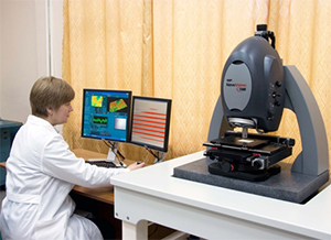
Optical profilometer (interferometer) of white light NewView 7300 (ZygoLOT, Germany). The device is designed for non-contact surface examination and thickness determination of film materials. It allows to form 2D and 3D profiles of samples surface and to analyse the obtained images. It is used to study the roughness of opaque substrates and to measure the height of the "step" formed by the sprayed material. The step height measurements are used to determine the sputtering speed of different materials.
Main characteristics:
|
Lithography section
|
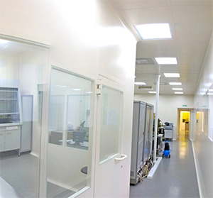
Hermetised clean room module for nanospintronics technologies. Used to locate and operate technological, lithographic and analytical equipment.
Main characteristics:
|
|
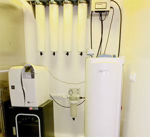
The Elix 10 Milipore ultrapure water treatment system is designed to produce reagent-grade ultrapure water for use in the lithography cycle.
Main characteristics:
|
|
Exposure and alignment setup MJB4 (SUSS Micro Tec., Germany). Designed for UV light illumination of photoresist using masks in the tasks of contact photolithography.
Main characteristics:
|
|
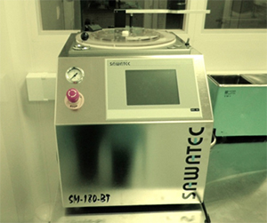
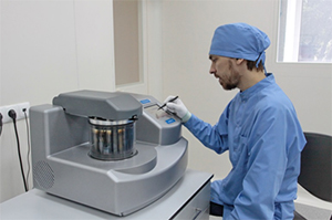
Sawatec SM 180 laboratory centrifuge (Sawatec Solutions, Liechtenstein). Designed for the application of homogeneous resist films by centrifugation at speeds up to 10'000 rpm.
Main characteristics:
|
|
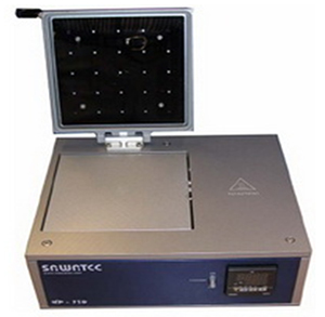
Sawatec HP-150 temperature table (Sawatec Solutions, Liechtenstein). The temperature table allows heating plates and substrates with high uniformity. It is used for drying photoresist, drying epoxy coatings, as well as for any other work that requires maintaining a precise heating temperature.
Main characteristics:
|
|
Semi-automatic ultrasonic microwelding unit HB16 ("TPT Wire bonder", Germany). Creation of wire leads or jumpers in microcircuits by ultrasonic resistance welding.
Main characteristics:
|
|
Cascade PM5 probe station (Cascade Microtech GmbH, USA). Designed for measurements of electrical properties of spintronic devices and chips on wafers and substrates up to 150 mm in size.
Main characteristics:
|
|
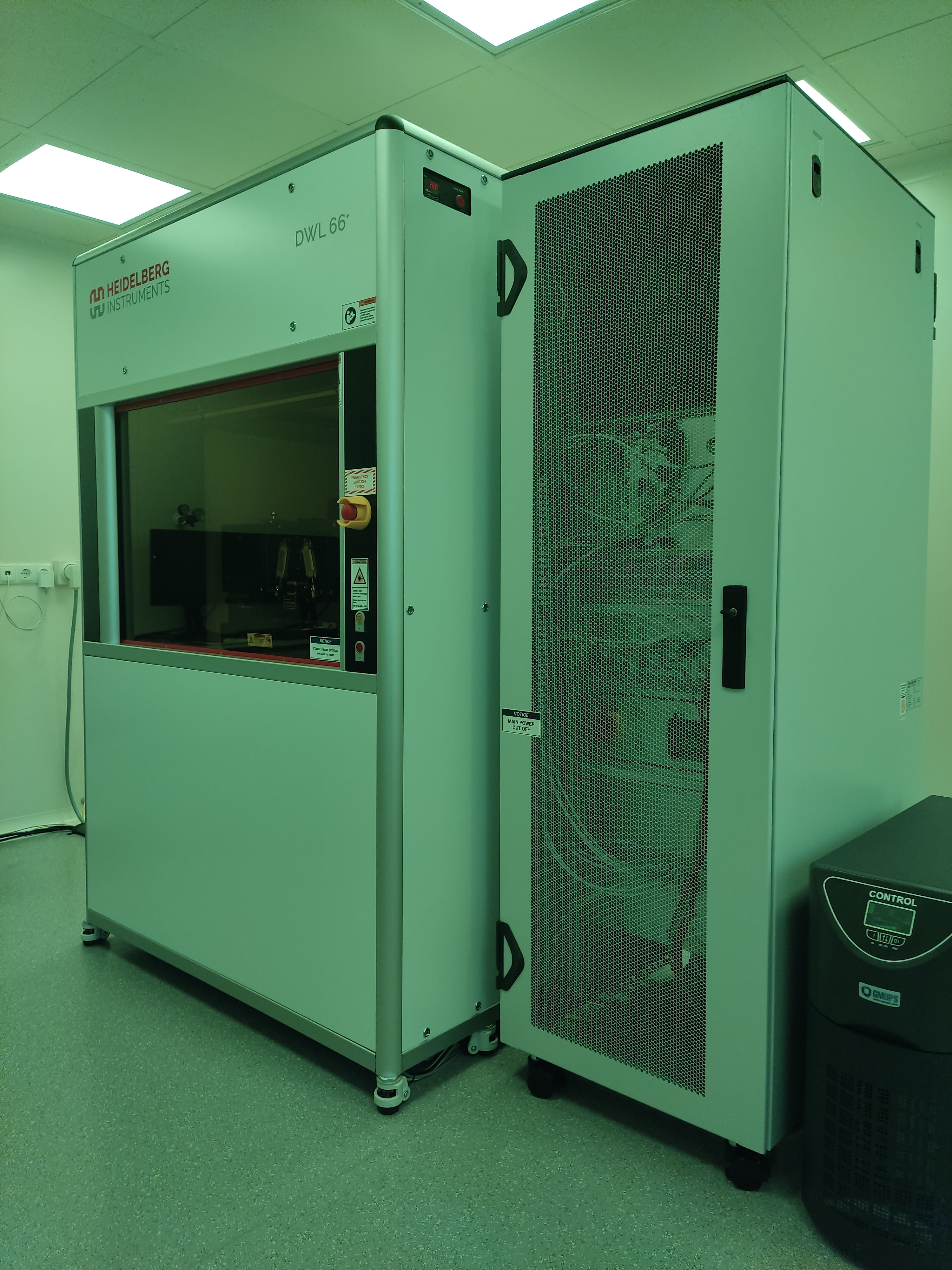
DWL66+ maskless laser lithography unit (Heidelberg Instruments Mikrotechnik GmbH, Germany). Designed for direct image formation on photoresist using diode laser (405 nm, 300mW).
Main characteristics::
|
Analytical equipment
|
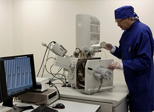
Inspect F raster scanning electron microscope (FEI Company) with a field autoemission cathode and Raith electron beam lithography system. It is designed for imaging of various objects with magnification exceeding 100'000x, as well as for imaging of micro-objects by means of programmable illumination of the electron resist layer with a focused electron beam. It is additionally equipped with an AMETEK APOLLO energy dispersive X-ray spectrometer with the EDAX GENESIS SPECTRUM system, which enables X-ray microanalysis of massive and film materials from chemical element B to U.
Main characteristics:
|
|
Table-top metal and carbon sputtering unit Q 150T ES (Quorum Technologies, UK). The unit is designed for vacuum deposition of metal films for lithographic tasks (metallisation of conductive tracks and contact pads), as well as for creation of thin carbon films on the surface of non-conductive samples used in electron microscopic studies.
Main characteristics:
|
|
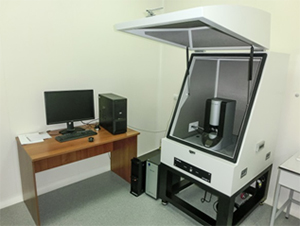
Automated scanning probe microscope "Solver Next" (produced by NT-MDT CJSC, Russia), designed to determine physical and chemical properties of objects with high spatial resolution using scanning atomic force and tunnelling microscopy techniques. This device is used for characterisation of obtained and investigated nanomaterials and nanostructures (including metallic magnetic films, planar nanostructures, etc.).
High spatial resolution:
|
|
Automated X-ray diffractometer DRON-3M (Burevestnik, Russia) is designed for a wide range of X-ray diffraction studies of various samples. It is used for X-ray diffraction imaging in small (2θ = 0.2° ÷ 12°) and large angles, as well as texture studies of film samples.
Main characteristics:
|